

Plug-in connection end插接式端头
The end uses a plug-in form, with clearance arranged for insertion, removal and cable bends.端头采用插接形式,可围绕安装位置安排插入、退出及线缆弯曲空间。
LVDS Dual Multi-Pin Connectors Jacketed Display Cable combines plug-in connection end, molded-end outline. Interface, circuit and installation data guide dimensions, material selection and sample review.LVDS双多针接头包覆屏线的结构重点包括插接式端头、包覆端头轮廓。接口、电路与安装资料将作为尺寸、物料和样品制作的确认依据。
Use the lvds dual multi-pin connectors jacketed display cable form as a starting point and confirm these design points against drawings and the actual equipment.以LVDS双多针接头包覆屏线的结构形式为起点,结合图纸和实际设备确认以下设计要点。
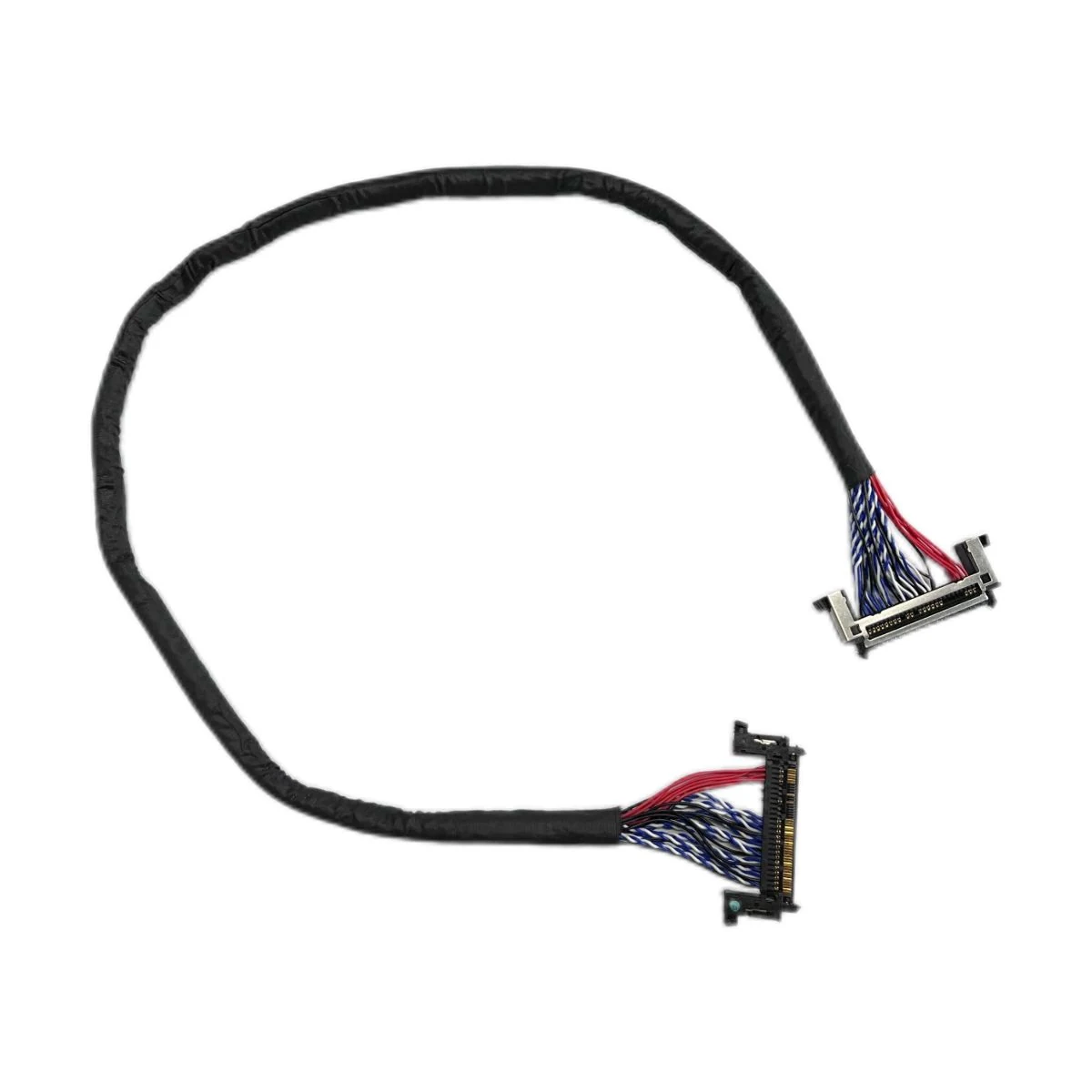
The end uses a plug-in form, with clearance arranged for insertion, removal and cable bends.端头采用插接形式,可围绕安装位置安排插入、退出及线缆弯曲空间。
The end transition has an overmolded form. Its outline can be configured around mating access and cable-turn clearance.端头过渡段具有包覆形态,可围绕接口插拔和线缆转向空间调整外部轮廓。
Define signal type, pair allocation, shield continuity and termination as well as the connector shape. Establish transmission performance from the actual cable, length and system validation.在接口外形之外确认信号类型、线对分配、屏蔽连续性和端接方法;传输能力应按实际线材、长度及整机验证结果确定。
Select conductors and insulation from circuit loads, diameter limits, bending and exposure. A material name does not replace ratings or validation results.从电路负载、外径限制、弯曲方式与环境条件选择导体和绝缘体系;材料名称不应直接代替额定参数或验证结果。
Equal pin count can conceal different power assignments同针数屏接口可能具有不同供电针位
The table describes the construction and available configuration choices. Materials, dimensions, circuits and inspection requirements are agreed for each project.以下说明展示结构与可配置内容。具体材料、尺寸、电路和检验要求按项目确认。
| Panel/board interfaces and complete pin table面板、主板接口与完整针脚表 | Map panel and board ends by full interface references and pin tables.屏端与板端以完整接口型号和针图对应。 |
|---|---|
| LVDS channels, pair polarity and mappingLVDS通道、线对极性与映射 | Define differential channels and polarity separately from power assignments.差分通道、极性与供电分配分开定义。 |
| Backlight power and control circuits背光供电及控制回路 | Follow panel documentation for backlight, enable and dimming.背光、使能与调光配置遵循面板资料。 |
| Pair impedance, shielding and target length线对阻抗、屏蔽与目标长度 | Select pair construction, shielding and length for the transmission path.线对结构、屏蔽和长度按传输路径选配。 |
| Circuit and revision reference电路与版本依据 | Confirm transmitter and receiver part numbers; connector drawings and pin map; pair count and lane assignment; target differential impedance; data rate and clock; cable length and routing; power/backlight circuits; shield and ground strategy; mechanical movement; sample and validation limits.需要确认发送端与接收端型号、连接器图纸和针脚表、线对数量与通道分配、目标差分阻抗、数据速率与时钟、线长和走线、电源/背光回路、屏蔽接地策略、机械运动、样品及验证限值。 |
| Sample and manufacturing configuration样品与制造配置 | After interface and signal requirements are frozen, engineering reviews the interconnect stack, prepares controlled samples, verifies electrical continuity and the agreed high-speed performance, then releases drawings, BOM, tooling and inspection points for repeat production.接口与信号要求冻结后,工程团队审核完整互连链路,制作受控样品,确认电气导通与约定的高速性能,再放行图纸、BOM、工具和检验点用于重复生产。 |
These are connection directions for project discussion. Suitability depends on interfaces, circuits, installation conditions and project validation; configuration can be adapted to the equipment.以下为可讨论的连接方向。实际适用性取决于接口、电路、安装环境和项目验证,可按设备需求调整。
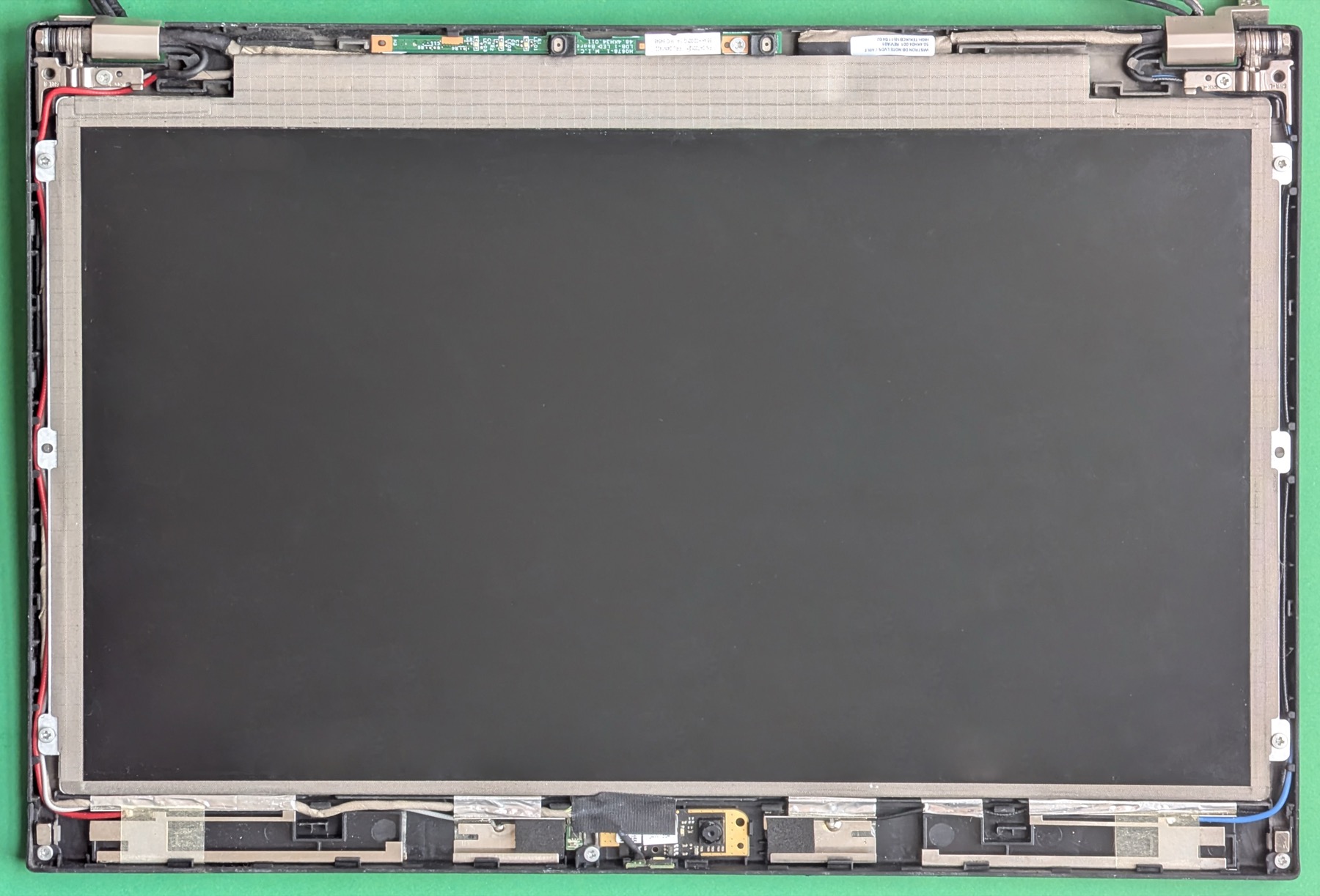
Confirm panel/board channel mapping separately from backlight circuits. Map panel and board ends by full interface references and pin tables.显示面板与主板的通道映射及背光分别确认。选配时,屏端与板端以完整接口型号和针图对应。
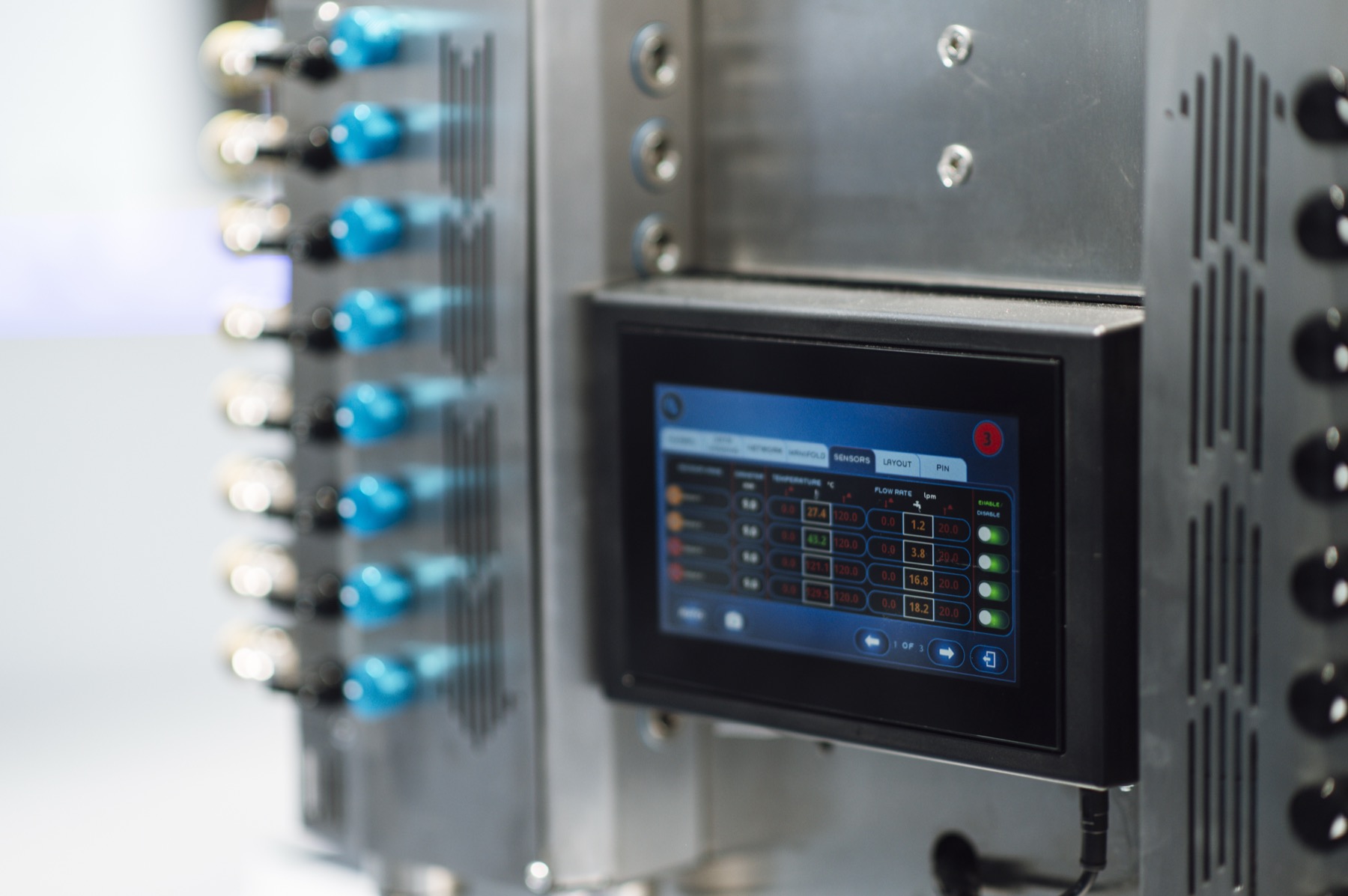
Coordinate bends, fixing and interface direction in thin spaces. Define differential channels and polarity separately from power assignments.薄型安装空间需要协调弯曲、固定和接口方向。选配时,差分通道、极性与供电分配分开定义。
Define signals and power from panel documentation and the actual board. Follow panel documentation for backlight, enable and dimming.以面板资料和实际主板定义信号及供电。选配时,背光、使能与调光配置遵循面板资料。
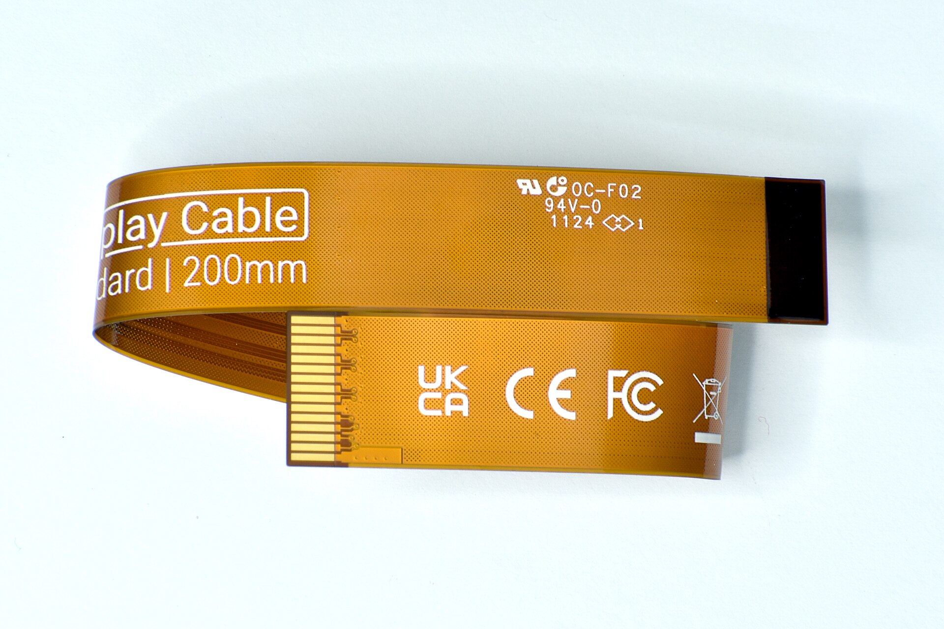
Match connector height, insertion direction and differential channels. Select pair construction, shielding and length for the transmission path.连接器高度、插入方向与差分通道同时匹配。选配时,线对结构、屏蔽和长度按传输路径选配。
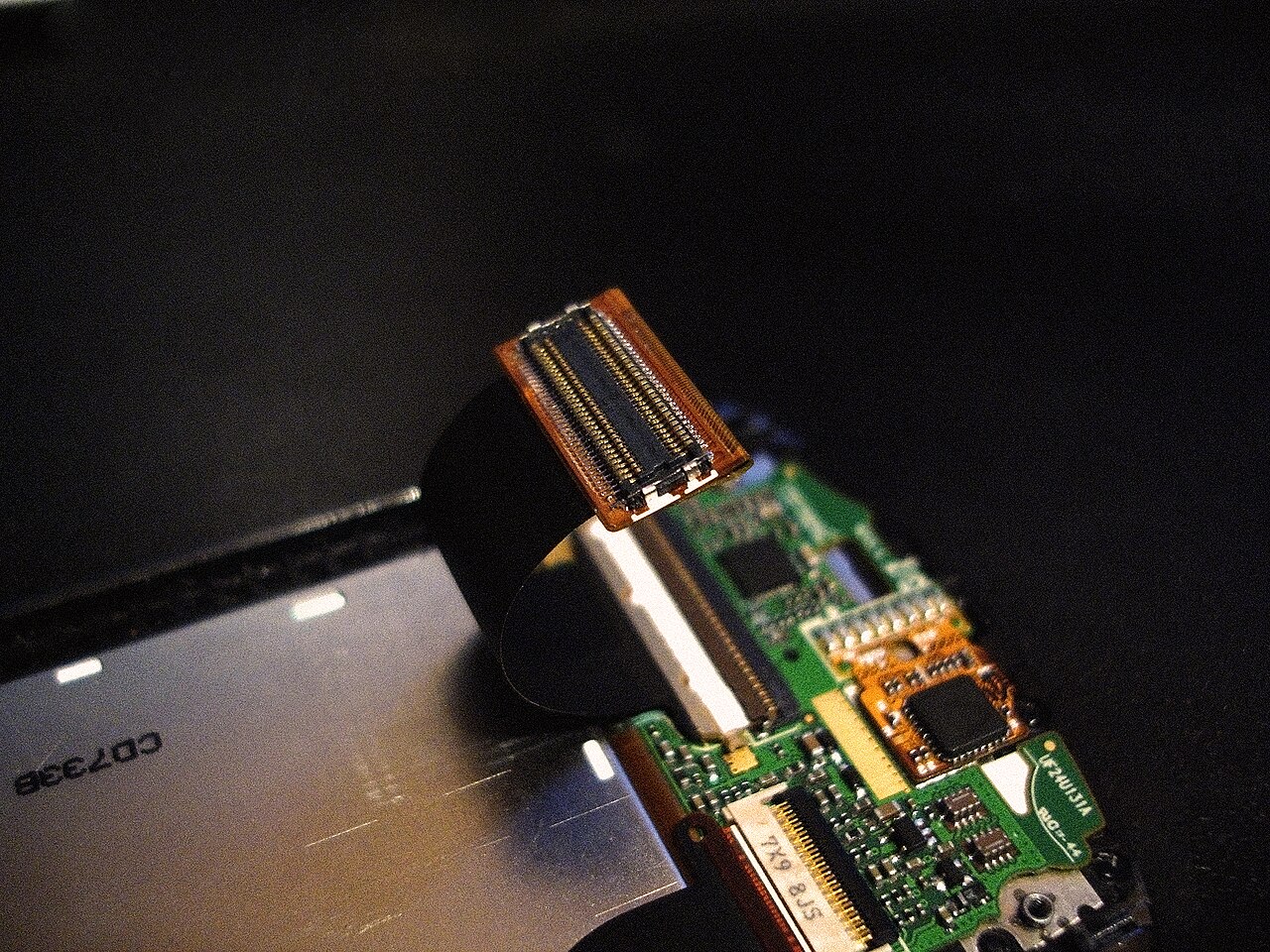
Check power and signal assignments even for equal-pin-count panels. Map panel and board ends by full interface references and pin tables.同针数面板仍需逐项核对供电与信号排列。选配时,屏端与板端以完整接口型号和针图对应。
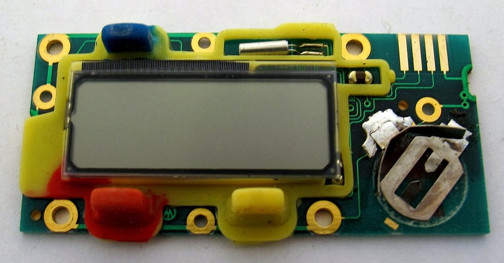
Avoid termination strain in short bends, clamps and shield transitions. Define differential channels and polarity separately from power assignments.短距离折弯、夹持与屏蔽过渡应避免端头受力。选配时,差分通道、极性与供电分配分开定义。
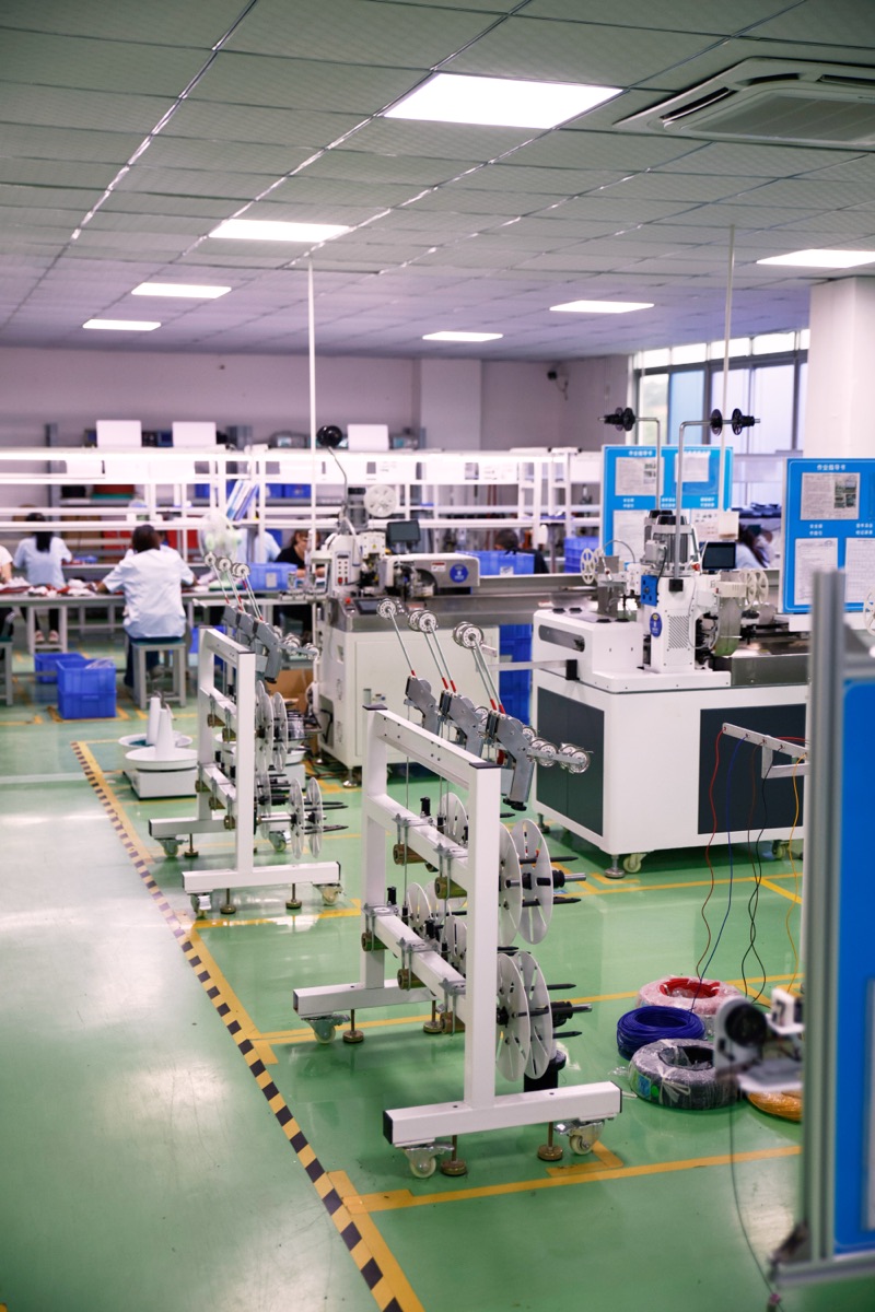
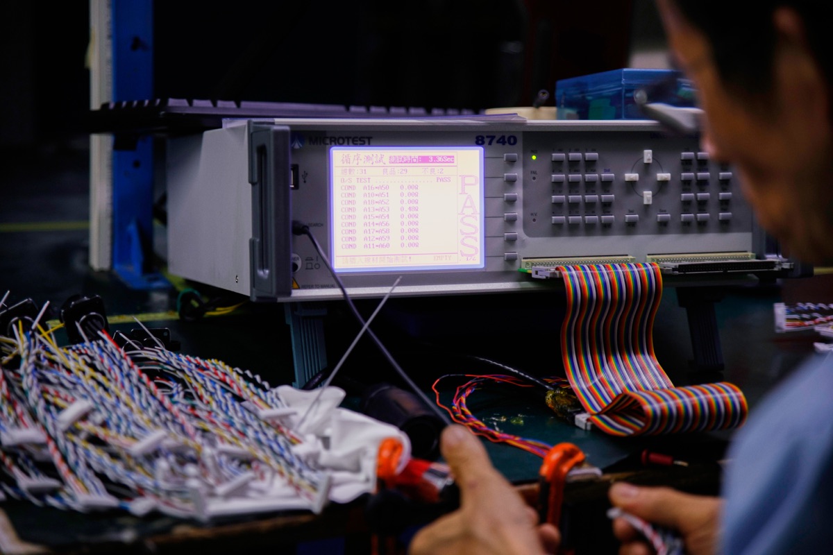
Our China factory supports lvds cable assembly projects through custom wire harness manufacturing and OEM/ODM development. Interface, circuit and installation data guide material selection, sample builds and manufacturing-document approval before repeat production.Super Smile-Tech 中国工厂围绕LVDS电缆组件的项目需求提供定制线束制造与 OEM/ODM 支持。我们从接口、电路与安装资料开始,协同物料选配、样品制作和制造文件确认,再按批准要求组织重复生产。
Map panel and board ends by full interface references and pin tables.屏端与板端以完整接口型号和针图对应。
Define differential channels and polarity separately from power assignments.差分通道、极性与供电分配分开定义。
Select pair construction, shielding and length for the transmission path.线对结构、屏蔽和长度按传输路径选配。
No. Displays may use LVDS, eDP, MIPI, FPD-Link, GMSL or proprietary parallel/serial interfaces. Connector appearance alone cannot identify the electrical interface.不是。显示系统可能使用 LVDS、eDP、MIPI、FPD-Link、GMSL 或专用并行/串行接口,仅凭连接器外观无法判断电气接口。
A sample helps with connector, length and routing, but data rate, pin map, pair assignment, impedance, termination, shield grounding, power circuits and acceptance limits still require equipment data or engineering confirmation.样品有助于确认连接器、长度与走线,但数据速率、针脚表、线对分配、阻抗、端接、屏蔽接地、电源回路与接收限值仍需设备资料或工程确认。
No. Connector and board transitions, pair balance, length, loss, termination, stubs, grounding, crosstalk and the actual transmitter/receiver also affect the complete channel.不能。连接器与板端过渡、线对平衡、长度、损耗、端接、支路、接地、串扰及实际收发器都会影响完整通道。
Share mating interfaces, a circuit table, target lengths or a sample for the lvds dual multi-pin connectors jacketed display cable. We can use them to review configuration and sample requirements.提供LVDS双多针接头包覆屏线的对插接口、回路表、目标长度或参考样品,我们据此梳理选配与样品确认事项。